
2, 4, and 6-Layer PCB Stackup: Quick Guide to Choosing the Ideal Stackup
Why the stackup is your first critical decision
If the internal arrangement of copper, dielectrics, and planes is inconsistent, no cutting-edge microcontroller or top-notch firmware will save your project. An optimized stackup:
- Reduces EMI by up to 15 dB.
- Maintains 50 Ω impedances with narrow, manageable traces.
- Creates a low-inductance power distribution network (PDN) thanks to the capacitance between planes.
In short, it boosts reliability and speeds up certification.
2-layer PCBs – the starting point
Double-sided boards are still valid for simple prototypes or low-speed products. Typically, one side is used for signals and power; the other acts as a continuous ground plane.
| Side | Recommended use | Key to success |
|---|---|---|
| Top | Signals + VCC | Short traces, GND copper pours around. |
| Bot | Nearly solid GND plane | Stitching vias next to every layer change. |
Why it works The bottom plane provides current return within a few hundred microns, reducing loop inductance and crosstalk. GND pours on the top side further narrow the return path.
Limits and risks
- 50 Ω traces require ≥ 13 mil: density drops by half compared to thinner boards.
- Point-to-point VCC distribution: requires more decoupling capacitors and careful voltage drop management.
- A ground plane interrupted by routes on the bottom side causes unexpected emissions.
When to move to 4 layers
When you need:
- Fine-pitch packages or BGAs.
- Frequencies above 50–80 MHz.
- Comfortable CE/FCC compliance margin.
4-layer PCBs – the new standard for startups
With four layers, you achieve an almost ideal balance between cost and performance. Allocating inner planes to ground and power is the big advantage.
Recommended stackup
- Layer 1: Signal + components.
- Layer 2: Solid GND.
- Layer 3: VCC (or second GND if EMI is a priority).
- Layer 4: Signal + minor components.
Key benefits
External signals always “see” a nearby reference plane, maintaining signal integrity and minimizing radiation. The reduced separation between VCC and GND on layers 2–3 creates distributed capacitance that absorbs current transients.
Mistakes to avoid
- Using all four layers for routing: wastes the chance for solid planes and generates noise.
- Separating GND and VCC with a thick core: increases PDN inductance.
- Lack of return vias when changing layers: opens loops and spikes EMI.
For most professional MVPs, this 4-layer stack simplifies design and reduces iterations.
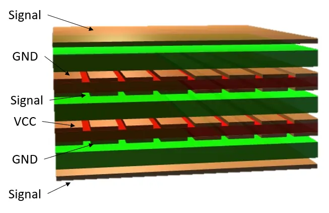
6-layer PCBs – extra power and silence
When pin count, speed, or multiple voltages increase, six layers offer room without compromising integrity.
Typical stackup
- Signal
- GND
- Signal (stripline)
- VCC
- GND
- Signal
Each signal layer is adjacent to a reference plane, containing EM fields and stabilizing the PDN. Also:
- Up to four routing layers make escaping 0.5 mm BGAs easier without blind vias.
- The VCC–GND pair (layers 4–5) adds planar capacitance, reducing the need for discrete high-frequency capacitors.
- Outer layers can be copper-filled to GND to shield the entire board.
Additional cost ≈ 30–40% over a 4-layer board, justified if you need high density, low emissions, or certification headroom.
Quick comparison
| 2 layers | 4 layers | 6 layers | |
|---|---|---|---|
| Impedance control | Difficult, traces ≥ 13 mil | Easy, ≈ 6 mil | Very easy, ≈ 4 mil |
| Expected EMI | High | Medium-low | Very low |
| Power distribution network (PDN) | Traces + many decoupling caps | VCC plane close to GND | High planar capacitance |
| Density and fan-out | Limited | Medium-high | Very high |
| Relative cost | 1× | ~1.4× | ~1.9× |
Conclusion: the stackup decides your success
A consistent stackup is the foundation of a reliable PCB. Use 2 layers only for simple, slow designs. Adopt 4 layers for most professional products. Move to 6 layers when speed, EMI, or density demand it.
Ready for a winning stackup?
At InnovaPCB we turn these concepts into boards that pass tests the first time. Contact us and discover how we can accelerate your development and shield your product from EMI.