
Practical Guide to PCB Antenna Design and Tuning: Trace, Chip, and Patch
Introduction
In an increasingly connected world, the efficiency of wireless communication has become a critical factor in the design of embedded devices. Whether for IoT, wearables, or industrial sensors, choosing and optimizing the right antenna on a printed circuit board (PCB) makes the difference between a reliable product and one prone to failure or limited range.
Types of Antennas for Connectivity and Their Advantages
-
PCB Trace Antenna (Inverted-F, monopole, dipole):
- Advantages: No additional cost, fully integrated, ideal for low-volume production.
- Disadvantages: Sensitive to layout and surroundings, requires fine tuning.
-
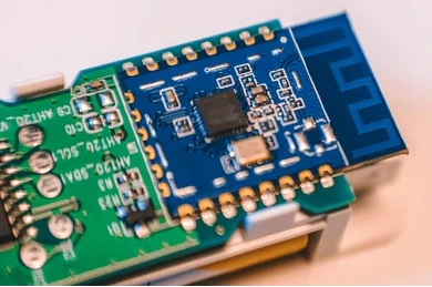
Chip Antenna (ceramic):
- Advantages: Compact size, factory pre-tuned, less sensitive to surrounding elements.
- Disadvantages: Lower efficiency, higher unit cost, requires external matching.
-
Patch Antenna:
- Advantages: Controlled directionality, ideal for GNSS and high-performance applications.
- Disadvantages: Requires more space, best suited for high frequencies.
-
Helical and External Antennas:
- Advantages: Good trade-off between size and gain, mechanical flexibility.
- Disadvantages: Additional cost, requires connector or manual assembly.
Criteria for Antenna Selection
When designing an antenna, consider:
- Operating frequency: For example, 2.4 GHz corresponds to a 125 mm wavelength. A quarter-wave antenna will be about 31 mm long.
- Size and form factor: Available space and position free from metal or dense plastics.
- Power vs performance: Passive antennas need fine tuning to maximize efficiency.
- Usage environment: Indoor (walls), outdoor (weather), vehicles (shielding).
Best Practices by Antenna Type
PCB Trace Antenna
- Keepout area: At least 6 mm copper-free around the antenna.
- Track width: Calculated for 50 ohms (microstrip or coplanar), adjusted to the layer stack.
- Ground plane: Avoid ground beneath the radiating element. Use a continuous ground under the feed line.
Chip Antenna
- Ground clearance: No copper underneath; typically needs a 10x10 mm free zone.
- Matching: LC network with components like 1 nH inductor + 2–5 pF capacitor.
- Positioning: Place at edges or corners, away from large copper areas.
Patch Antenna
- Dielectric substrate: Use low-loss materials like Rogers or Taconic.
- Polarization: Linear or circular depending on application.
- Feeding: Slot coupling or coaxial connection. Ensuring 50-ohm impedance at the feed point is essential.
Simulation, Measurement and Tuning
Simulation Tools
- HFSS, CST, ADS: Full 3D electromagnetic analysis.
- MATLAB Antenna Toolbox: Parametric design and radiation pattern simulation.
- Open source tools: QucsStudio, KiCAD with RFTools, Antenna Magus (student edition).
Measuring with a Vector Network Analyzer (VNA)
To evaluate antenna performance, a VNA measures scattering parameters, especially S11, which indicates the reflection due to impedance mismatch.
Basic measurement steps:
- Calibration: Use a standard SOLT kit (short, open, load, thru) to eliminate errors from cables and connectors.
- Setup: Connect the antenna using U.FL, SMA or similar test connector. Keep cable length minimal to reduce loss.
- S11 parameter reading: The VNA plot shows a dip at the antenna’s best match frequency (ideally S11 < –10 dB or VSWR < 2).
- Analysis: If the dip does not match the target frequency (e.g. 2.4 GHz), adjust the antenna physically or via components.
Practical Tuning
Tuning aligns the antenna resonance and impedance with the desired frequency. Common methods include:
- Track trimming: Design slightly longer and trim by millimeters after testing until resonance is achieved.
- Adding copper bridges: Extend the effective length to lower the resonance frequency.
- Using passive components: Matching networks (Pi or T) using inductors and capacitors—e.g., 3 pF series cap, 1 nH shunt inductor, 2 pF series cap.
- Feed point repositioning: In patch antennas, adjust feed location to match 50 ohms.
After each adjustment, re-measure using the VNA to verify tuning accuracy.
Quick Comparison of Antennas
| Feature | PCB Trace Antenna | Chip Antenna | Patch Antenna |
|---|---|---|---|
| Size | Integrated in PCB | Very compact | Requires more area |
| Cost | Low | Medium-high | Medium |
| Efficiency | High (if well tuned) | Medium | High |
| Tuning difficulty | High (physical trimming) | Medium (via matching) | Medium (by feed position) |
| Environment sensitive | Yes | Moderately | Yes |
| Directionality | Omnidirectional | Omnidirectional | Directional |
Designing antennas on PCBs is a balance between performance, space and cost. By applying these principles, you can build wireless devices that are robust and efficient from prototype to production.
If you’re planning a PCB with wireless connectivity and want to follow best practices in routing, impedance matching, and tuning, contact us at innovaPCB. Our team provides expert guidance in PCB design and firmware development for optimal wireless performance.