
Configurable Logic Peripheral (CCL/CLB): concept, architecture and use cases
Summary
Generating precise timing signals in microcontrollers often requires bit‑banging, i.e. having the CPU devote entire cycles to toggling pins with nanosecond accuracy, which limits the time available for other tasks. Configurable logic peripherals—also known as CCL, CLC, CLB, UDB, among others—allow these functions to be off‑loaded to hardware, achieving deterministic response and freeing processor resources.
These programmable logic blocks integrated into the microcontroller use LUTs (truth tables), flip‑flops and internal signal paths to create logic gates, timers and state machines that operate autonomously, without CPU intervention. This enables latencies of only a few nanoseconds and allows them to operate even in low‑power mode. The result is real‑time execution, reduced firmware load and the possibility of eliminating external components, simplifying the design and
1. What is a CCL/CLB peripheral?
Essentially, a CCL/CLB is a LUT‑based logic array.
Each LUT stores a truth table for up to 3–4 signals; its output can be registered in a flip‑flop and routed to other LUTs, internal peripherals or I/O pins.
Unlike a full FPGA, the number of logic cells is small—on the order of tens—but enough to “glue” signals, generate pulses or implement simple state machines.
1.1 Operating philosophy
- Multiple inputs: pins, timer outputs, SPI/UART buses, internal clocks, even register bits.
- Combinational logic: the LUT evaluates the truth table every clock cycle.
- Sequential logic: D, JK flip‑flops or latches allow states to be stored, frequencies to be divided and counters or state machines to be built.
- Timing blocks: small counters, debounce filters and edge detectors eliminate glitches and generate precise pulses.
- Flexible routing: crossbars or event systems link the outputs with other peripherals to trigger ADCs, reset timers or switch PWM, with no software in between.
2. Typical internal blocks
| Block | Main function | Note |
|---|---|---|
| LUT (1–4 inputs) | Implements any logic gate by means of a truth table | Usually 2–32 per device. |
| Flip‑flops / Latches | Store the LUT result on an edge or level, useful for dividers, D/JK/T FFs | |
| Short counters | Generate delays or time windows of a few cycles | Normally 3–8 bits. |
| Edge detectors | Turn transitions into fixed‑width pulses; vital for debouncing | |
| Filters / Synchronizers | Align asynchronous signals to the CCL clock and filter glitches | |
| Crossbar / Event System | Switching network that connects logic inputs and outputs with other peripherals (timers, ADC, GPIO) | |
| Routes to GPIO pins | Allow the logic signal to be exposed externally without occupying CPU |
3. Typical applications
- Glue logic: replacing 74HC ICs with internal programmable gates.
- Single‑wire communication drivers (e.g. WS2812 LEDs, IR protocols) generated entirely in hardware.
- Quadrature decoders or encoders for motors, with no CPU latency.
- Autonomous button filtering and timing (debounce).
- Exotic PWM or modulation generators to turn basic timers into advanced controllers.
- Small finite‑state machines that react to critical events within nanoseconds.
- Fast clock dividers and counters useful in frequency‑measurement applications.
4. Key advantages
- Deterministic real time: the logic runs in parallel with the CPU with delays ≪ 1 µs, ideal for critical signals.
- Lower firmware load: frees processor cycles and avoids complex interrupts.
- Reduced component count: external gates, dedicated drivers or CPLDs can disappear, simplifying the PCB and lowering costs.
- Optimized power: the logic keeps running in Sleep, cutting mA in IoT or portable applications.
Comparison with other embedded logic technologies in microcontrollers
| MCU family / Manufacturer | Programmable logic technology | Available logic resources | Configuration flexibility | Ease of use (tools) |
|---|---|---|---|---|
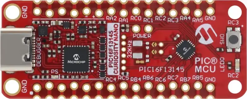
| Microchip PIC16F13145 (8‑bit PIC) | CLB – Configurable Logic Block (formerly CLC – Logic Cell) | ~32 BLEs (4‑input LUTs each with FF) in 4 logic cells; integrated 3‑bit counter. | Allows basic combinational and sequential logic inside the MCU. Integrates with many internal peripherals and I/O pins (PPS), supports run‑time dynamic configurations. Ideal for implementing gates, flip‑flops, one‑shots, small state machines, pulse generators, etc. | High – Microchip offers a graphical tool (MPLAB Code Configurator / CLB Synthesizer) to design the logic schematically or by importing Verilog modules. Moderate learning curve but good documentation and examples. |
| TI C2000 (32‑bit MCUs aimed at digital control) | CLB – Configurable Logic Block (C2000) | Several logic blocks per chip (e.g. 4 tiles). Each CLB tile includes 3‑ to 4‑input LUTs, multiple programmable state machines (FSM) and counters up to 32 bits, interconnected via a configurable matrix. | Very high – Designed to extend real‑time control peripherals. Can implement complex combinational logic and advanced sequential logic (e.g. motor control, encoders, specialized serial protocols) without external FPGA. The CLB can take internal/external signals via crossbar and drive pins or modules. | Medium – Texas Instruments provides a configuration tool (CLB Tool) integrated into its IDE (CCS). Logic can be designed graphically and loaded into the MCU. Documentation is complete, but using the CLB may require familiarity with digital design concepts. |
| Infineon/Cypress PSoC 4/5 (ARM Cortex‑M) | UDB – Universal Digital Blocks | Up to several UDB units per micro (e.g. 4 in PSoC4, 24 in PSoC5). Each UDB contains 2 small PLDs (programmable logic macrocells) + an 8‑bit datapath (ALU, registers, FIFO). Interconnection via digital signal matrix (DSI). | Very flexible – UDBs allow creation of both custom combinational logic and complete digital components (UARTs, extra timers, PWMs, communication controllers, etc.). Blocks can be chained for larger functions. Practically any small‑scale digital circuit (up to 8 bits) can be implemented in these programmable blocks. | Medium/High – Uses PSoC Creator environment, with schematic design or simple HDL code. Low learning curve for simple functions (dragging predefined logic components) but increases if designing complex logic from scratch. Integration with firmware is smooth via auto‑generated APIs. |
| STMicroelectronics STM32 (various ARM Cortex‑M series) | (No dedicated logic block) Use of generic peripherals (Timers + DMA) | N/A (no generalized programmable LUTs). Advanced timers, DMA controllers, triggers and interrupt/event routing are leveraged to achieve logic functions. E.g. timer + DMA to generate pulse trains with timed GPIO patterns. | Limited – Although there is no “internal FPGA”, certain patterns and peripheral links can emulate discrete logic. Example: using a timer in PWM mode to form a pulse and chaining DMA to update its duty cycle bit by bit, achieving a WS2812‑style signal without CPU intervention. However, flexibility is lower compared to dedicated LUTs; limited to what timers, comparators and DMAs allow (aimed at waveform generation, signal demodulation, etc.). | Low – There is no specific GUI for “configurable logic”. Implementation is done by manually configuring standard peripherals using tools like STM32CubeMX (e.g. setting a TIM with DMA and routing signals). Achieving certain functions requires creativity and deep knowledge of the modules (e.g. exploiting timers and DMAs in unusual modes), so implementation is less straightforward. |
Practical example: WS2812 LED strip driver
For the WS2812 protocol (~800 kHz), a classic firmware running on a PIC would consume almost 100% of the CPU. With the CLB a few LUTs and an internal counter are enough: the micro’s SPI sends the bit stream and the configurable logic gives it the exact pulse width. See the step‑by‑step implementation in the repository pic16f13145‑spi‑ws2812 and in the All About Circuits article for full details.
In practice, this circuit allows the WS2812 LED strip to be driven almost entirely in hardware: the programmer simply loads the color data into the SPI buffer (for example using DMA, or in a loop while the previous transmission is still in progress) and the configurable logic takes care of timing and formatting it correctly.
Conclusion
CCL/CLB peripherals place programmable logic right where it is most needed: inside the microcontroller. They offer minimal latency, operate independently of the CPU and suppress external components, leading to more compact and cost‑effective designs.
Want to leverage this technology in your next project?
Get in touch with InnovaPCB: we design tailor‑made embedded solutions, implement logic drivers and optimize your hardware to achieve maximum efficiency and reliability.